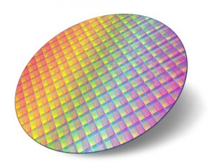
Semiconductor Diffusion Furnaces

Semiconductor device processing is highly demanding of film uniformity and low defect density. Expertech has over 25 years of experience providing innovative equipment and process support for semiconductor applications. Whether you need to introduce a new film type or need to augment production capacity for an existing process, Expertech can provide a solution.
Expertech can provide one or more horizontal or vertical furnace systems configured for doing the following semiconductor device processing steps:
LPCVD Processes
- Stochiometric Nitride (Si3N4)
- Anti-reflection coatings (ARC)
- Low Stress Nitride (Si Rich Nitride) < 250 MPa
- Ultra-low Stress Silicon Nitride < 100 MPa
- Undoped Polysilicon or α-Silicon
- Phosphorous Doped Polysilicon or α-Silicon
- Boron Doped Polysilicon or α-Silicon
- Undoped Poly-SiGe
- Phosphorous or Boron Doped Poly-SiGe
- Undoped Low Temperature Oxide (LTO)
- Phosphorous Doped Glass (PSG)
- Boron and Phosphorous Doped Glass (BPSG)
- Undoped deposited oxide by TEOS
- Phosphorous Doped TEOS Oxide (PSG)
- Boron and Phosphorous Doped TEOS (BPSG)
Atmospheric Pressure Processes
- Wet or Dry Oxidation/Densification
- Dry/wet/dry Gate Oxide Cycles
- Inert Gas Anneals/Densification (N2, Ar, He)
- Contact Sintering / Alloy (N2, Forming Gas)
- Reducing Atmosphere Anneals (Forming Gas)
- Phosphine + O2 phosphorus doping
- Phosphine gas phase doping
- POCl3 + O2 – liquid source phosphorus doping
- BBr3 + O2 – liquid source boron doping
- Solid Source Phosphorous Doping
- Solid Source Boron Doping
- Drive-in / Redistribution
